The red led turns for the channel I am sending the signal to, the manual says that red led means DDS synchronization/ pll error.
DDS-Testing
Why did you set pll_en to 0?
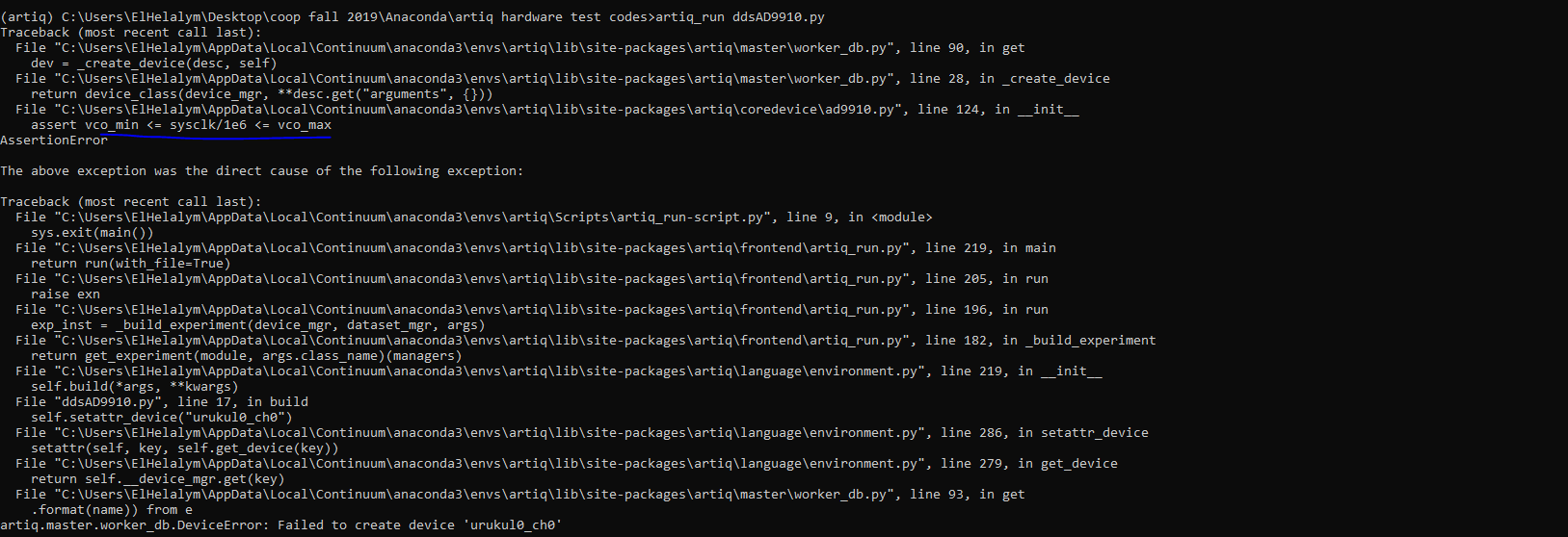
I miss read the pll_en parameter on the artiq website, I thought pll_en:1 bypassed the pll, but thats the default. I fixed that in the device data file, and now I am getting the Vc0 min < sysclock/1e6 < Vco max error. I am using Vco1 range which is from 420 to 590 MHz, and using both a 50 and 42 multiplier and a 10MHz external clock, the range is then 8.4 < sysclock<11.8 for 50 , and 10< sysclock<14 MHz. I am still however getting the same the Vc0 min < sysclock/1e6 < Vco max error message. Is there a certain VCO 1-5 range that our NRC board comes fixed with or can I choose.

Just to clarify, I used 42 multiplier and got the vco error message, So then I tried 50 multiplier and got the same error message
You can choose the VCO range using the pll_vco parameter.
okay I did that, I am using Vco1 range which is from 420<sysclock< 590 MHz, multiplier of 45 and a 10MHz external clock and I am still getting a vco range error ?
Read the ad9910 source.
You may also want to verify using the datasheet whether the loop filter will work for what you want to do.
I did read the ad9910 data sheets, from my understanding using Vco1 range which is from 420<sysclock< 590 MHz, multiplier of 45 and a 10MHz external clock , the driving external clock falls in the the 9.3(420/45) < 10Mhz <13.1Mhz,
rjo all I am doing is trying to turn this code on an external 10Mhz clock rather than the internal 125Mhz one.
from artiq.experiment import *
import numpy as np
class DDSTest(EnvExperiment):
def build(self):
self.setattr_device("core")
self.setattr_device("urukul0_ch0")
@kernel
def run(self):
self.core.reset()
self.urukul0_ch0.set_att(0dB)
self.urukul0_ch0.init()
self.urukul0_ch0.sw.on()
self.urukul0_ch0.set(10MHz,1.0,1.0)
delay(3000000*ms)
self.urukul0_ch0.sw.off()
The algorithm that raises the VCO error is simple and should be easy to understand and debug. https://github.com/m-labs/artiq/blob/f2f7170d20709c77b2521f27fe8141dda86df006/artiq/coredevice/ad9910.py#L122-L124
Hmm. I'm not sure you understand the requirements. Assuming you did read the datasheet, what phase margin and loop bandwidth do you expect in the use case you describe?
rjo phase margin and bandwidth parameters allow for optimization, I do not need to include them in my device_dp.py file. From my understanding the only parameters that need adjustment are the following pll_n":42 ,(Multiplier) "pll_vco":1 (VCO range), "pll_cp":7,refclk": 10000000.0 ( Frequency of the external clk) "clk_sel": 1 (Connects to external clock ) and they need to be changed only in the device_dp.file, and according to sb10q and the test code remains unchanged. If I am missing something please clarify
You are actively resisting advice. If you don't respect the help you get, you won't get very far.
- As I said I am unsure whether this can work at all. But you refuse to check the loopfilter to verify that it will work on paper.
- The documentation clearly describes the clock divider in urukul. You'll need to take that into account.
I did not mean in anyway to resist the advice given, on the contrary I am trying to understand it (I am a student still and this is all new to me) . If you scroll back up I followed the instructions given by sb10q in terms of which parameters need to change in the device_dp file. from my reading phase margin and bandwidth are for optimization, https://www.analog.com/media/en/technical-documentation/data-sheets/AD9910.pdf . As for the multiplier, my understanding is that it my external clock (10MHz) has to fall between the correct VCO ( changed in device_dp using "pll_vco":1) range before its multiplied ( changed in device_dp using "pll_n":1). Is there another source I can read from to clear things up.
What phase margin and loop bandwidth do you expect in the use case you describe?
You need to calculate those values. If you can't, read up on PLL loop filters or have somebody else solve that for you. I haven't tried your use case and I'm not aware of anybody who has. You are on uncharted territory here and you need to follow the instructions to determine whether this works.
If you don't answer and insist on implying that these values are not relevant and reserved for optional optimization then I can't help you.
And the second question you haven't answered: What are you setting the urukul clock divider (clk_div) to?
I need you to look that up in the documentation and determine the value that is being used based on what you have in your device database. You need to answer that question.
Please stop pasting links and excerpts from files. Those don't answer the questions. I know what's in the datasheet and I know what you have pasted before. Repeating it doesn't help.